In the ever-evolving world of technology, the development of CMOS (Complementary Metal-Oxide-Semiconductor) stacked sensors has become a crucial advancement. These sensors are designed to enhance performance, reduce size, and improve energy efficiency in various applications. Two prominent methods for integrating these sensors are through the use of silicon interposers and copper hybrid bonding. This article aims to explore and compare these two techniques, highlighting their strengths and weaknesses.
**Silicon Interposers**

Silicon interposers, also known as silicon substrates, have been widely used in the semiconductor industry for many years. These interposers act as a layer between the sensor wafer and the back-end-of-line (BEOL) processes, providing a platform for integrating multiple sensors.
**Advantages of Silicon Interposers:**
1. **High Performance:** Silicon interposers offer excellent electrical and thermal properties, which enhance the overall performance of stacked sensors.
2. **Flexibility:** They allow for the integration of various types of sensors, including optical, thermal, and pressure sensors, on a single platform.
3. **Cost-Effective:** The manufacturing process for silicon interposers is well-established, making them a cost-effective choice for mass production.
**Disadvantages of Silicon Interposers:**
1. **Thick Structure:** The inclusion of a silicon interposer increases the overall thickness of the stacked sensor, which may limit its applicability in certain devices.
2. **Complexity:** The integration process for silicon interposers is more complex, requiring additional steps and equipment.
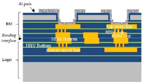
**Copper Hybrid Bonding**
Copper hybrid bonding is a relatively new technique for integrating CMOS stacked sensors. It involves bonding a thin copper layer to the sensor wafer, which acts as a bridge between the front-end-of-line (FEOL) and BEOL processes.
**Advantages of Copper Hybrid Bonding:**
1. **Ultra-Thin Structure:** Copper hybrid bonding allows for the creation of extremely thin stacked sensors, which is beneficial for applications with space constraints.
2. **High Throughput:** The bonding process is faster and more efficient than that of silicon interposers, making it suitable for high-volume production.
3. **Cost-Effective:** The use of copper reduces the manufacturing cost compared to silicon interposers.
**Disadvantages of Copper Hybrid Bonding:**
1. **Limited Material Compatibility:** Copper may not be compatible with all types of sensors, limiting the applicability of this technique.
2. **Thermal Conductivity:** Copper has lower thermal conductivity compared to silicon, which may affect the overall performance of the stacked sensor.
**Conclusion**
Both silicon interposers and copper hybrid bonding offer unique advantages and disadvantages for CMOS stacked sensors. The choice between these two techniques depends on the specific requirements of the application, such as performance, thickness, and cost.
As technology continues to advance, new methods and materials will likely emerge, providing even better options for integrating CMOS stacked sensors. However, for now, understanding the strengths and weaknesses of silicon interposers and copper hybrid bonding is essential for engineers and designers working in this field.