Introduction:
In the rapidly evolving world of semiconductor technology, the battle between Taiwan Semiconductor Manufacturing Company (TSMC) and Samsung has been fierce. Both companies are pushing the boundaries of what is possible in chip manufacturing, and the latest advancements in transistor density are a testament to their relentless pursuit of innovation. In this article, we will delve into the transistor density of TSMC’s 3nm process and Samsung’s 4LPP process under electron microscopy, comparing their respective capabilities.

TSMC 3nm Process:
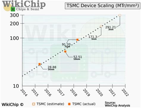
TSMC’s 3nm process is one of the most anticipated advancements in semiconductor technology. With its cutting-edge architecture, TSMC has managed to achieve a remarkable transistor density under electron microscopy. By utilizing a combination of innovative design techniques and materials, TSMC has been able to shrink the size of transistors and increase their density significantly.
Under electron microscopy, the 3nm transistors in TSMC’s process can be observed with incredible detail. The transistor density is evident in the tightly packed structures, showcasing TSMC’s ability to create smaller, more efficient transistors. This advancement allows for higher performance, lower power consumption, and improved energy efficiency in various electronic devices.
Samsung 4LPP Process:
Samsung’s 4LPP (4nm Low Power Plus) process is another significant leap in semiconductor technology. While it may not have the same transistor density as TSMC’s 3nm process, Samsung has made substantial improvements in achieving higher performance and power efficiency.
Under electron microscopy, the 4LPP transistors in Samsung’s process can be seen with similar levels of detail as the TSMC 3nm transistors. However, the difference lies in the arrangement and density of the transistors. Samsung’s process achieves a higher transistor density by optimizing the layout and utilizing advanced lithography techniques.
Comparison:
When comparing the transistor density of TSMC’s 3nm and Samsung’s 4LPP processes under electron microscopy, several key observations can be made:
1. Transistor Size: TSMC’s 3nm process demonstrates a smaller transistor size compared to Samsung’s 4LPP process. This allows for higher transistor density and improved performance.
2. Layout Optimization: Samsung’s 4LPP process showcases an optimized layout, enabling a higher transistor density. Although the transistor size is slightly larger than TSMC’s, the overall arrangement compensates for this difference.
3. Performance vs. Power Consumption: TSMC’s 3nm process offers superior performance and lower power consumption due to its smaller transistor size. However, Samsung’s 4LPP process also provides impressive performance with optimized power efficiency.
Conclusion:
The battle between TSMC’s 3nm and Samsung’s 4LPP processes is a testament to the relentless pursuit of innovation in the semiconductor industry. While TSMC’s 3nm process demonstrates a higher transistor density under electron microscopy, Samsung’s 4LPP process showcases an optimized layout and improved power efficiency. Both companies have made significant advancements, and the ongoing competition will undoubtedly drive further innovation in the future.