In the rapidly evolving world of semiconductor technology, the relentless pursuit of miniaturization and performance enhancement has led to the development of various transistor architectures. Among these, FinFET (Fin Field-Effect Transistor) has emerged as a game-changer, enabling the scaling of transistors beyond the limitations of traditional planar transistors. However, as we continue to push the boundaries of Moore’s Law, the scaling limits of FinFETs are being reached. This has prompted researchers to explore alternative transistor designs, and one such promising candidate is the 3D nanosheet transistor.
The 3D nanosheet transistor architecture is a novel design that offers several advantages over the FinFET. By stacking nanosheets vertically, this transistor design can achieve higher packing density and shorter channel lengths, thereby allowing for further scaling beyond the limitations of FinFETs. This article aims to explore the potential of 3D nanosheet transistors in surpassing the scaling limits of FinFETs and their potential impact on the semiconductor industry.

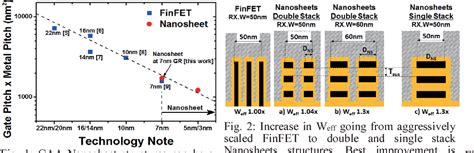
One of the key advantages of 3D nanosheet transistors is their ability to achieve shorter channel lengths. As transistors continue to scale down, the length of the channel becomes increasingly important in determining the transistor’s performance. In a FinFET, the channel length is defined by the thickness of the fin, which is limited by the manufacturing process. In contrast, 3D nanosheet transistors can achieve shorter channel lengths by stacking nanosheets vertically, thereby allowing for further scaling and improved performance.
Another advantage of 3D nanosheet transistors is their higher packing density. As the demand for more transistors on a single chip continues to grow, achieving higher packing density becomes crucial. By utilizing the vertical stacking of nanosheets, 3D nanosheet transistors can offer a significant increase in packing density compared to FinFETs. This can lead to more efficient and powerful integrated circuits (ICs) with reduced power consumption.
Moreover, 3D nanosheet transistors can also enhance the overall performance of ICs. Due to their shorter channel lengths and higher packing density, these transistors can achieve faster switching speeds and lower power consumption. This makes them highly suitable for high-performance computing and mobile devices, where energy efficiency and speed are critical factors.
Despite the numerous advantages of 3D nanosheet transistors, there are still challenges that need to be addressed. The manufacturing process for these transistors is more complex and requires advanced equipment. Moreover, the integration of 3D nanosheet transistors into existing fabrication processes may require significant modifications. However, as the semiconductor industry continues to invest in research and development, these challenges are likely to be overcome.
In conclusion, the 3D nanosheet transistor is a promising alternative to FinFETs, offering the potential to surpass the scaling limits of current transistor designs. With their ability to achieve shorter channel lengths, higher packing density, and improved performance, these transistors can revolutionize the semiconductor industry. As we continue to push the boundaries of technology, the 3D nanosheet transistor may well be the next step in the relentless pursuit of innovation and miniaturization.