In the ever-evolving landscape of technology, the race to create faster, more efficient, and powerful chips has become more intense than ever. This quest has led to the emergence of innovative technologies, with artificial intelligence (AI) playing a pivotal role. One such breakthrough comes from Google’s DeepMind, a division of Google focused on AI and machine learning. This article delves into how DeepMind is leveraging AI to optimize chip designs and revolutionize the semiconductor industry.
The Birth of DeepMind

Launched in 2014, DeepMind was initially focused on artificial general intelligence, which aims to create machines capable of performing any intellectual task that a human can. However, over the years, the company has shifted its focus to specialized AI applications, including medical research, gaming, and now, chip design.
DeepMind’s AI-Driven Chip Design Approach
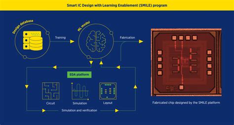
DeepMind’s approach to chip design is unique, as it relies on a combination of machine learning algorithms and neural networks to optimize circuitry. The process can be broken down into several key steps:
1. Data Collection: DeepMind first gathers vast amounts of data from existing chips and their performance metrics. This data includes various circuit configurations, material compositions, and process technologies.
2. Training: Using this data, DeepMind trains a neural network to identify patterns and relationships between different circuit components. This neural network can then predict the performance of new circuits based on their configurations.
3. Optimization: Once the neural network is trained, it is used to generate new circuit designs that optimize performance, power consumption, and area. These designs are then validated through simulations to ensure they meet the desired specifications.
4. Iteration: The process is iterative, with DeepMind refining the neural network and circuit designs over time to improve accuracy and efficiency.
The Benefits of AI-Driven Chip Design
The use of AI in chip design offers several advantages:
1. Efficiency: AI-driven design processes can significantly reduce the time and effort required to create new chips. This efficiency allows for faster product development and time-to-market.
2. Performance: By optimizing circuitry, AI can help create chips with improved performance, leading to faster and more efficient computing.
3. Cost: Optimized chip designs can also reduce the cost of manufacturing and power consumption, leading to more affordable and energy-efficient devices.
4. Innovation: AI-driven chip design opens the door to new possibilities, enabling the creation of chips with unique features and functionalities.
DeepMind’s Impact on the Semiconductor Industry
Google’s DeepMind has already made significant strides in the field of AI-driven chip design. Its technology has been applied to various semiconductor companies, leading to advancements in areas such as:
1. Data Centers: By optimizing the chip designs used in data centers, DeepMind’s technology can help reduce power consumption and increase processing speeds, making data centers more sustainable and efficient.
2. Consumer Electronics: AI-driven chip design can enhance the performance of consumer electronics, such as smartphones, laptops, and gaming consoles, providing users with better experiences.
3. Autonomous Vehicles: DeepMind’s technology can be used to design chips for autonomous vehicles, ensuring that these vehicles are safe, efficient, and capable of performing complex tasks.
Conclusion
As the demand for faster, more efficient, and powerful chips continues to grow, AI-driven chip design, especially with Google’s DeepMind, is set to revolutionize the semiconductor industry. By leveraging the power of machine learning and neural networks, DeepMind is paving the way for a new era of chip design, bringing innovation and efficiency to the forefront of technology.