Introduction:
The semiconductor industry is currently witnessing a fierce competition in the realm of Extreme Ultraviolet (EUV) lithography. Two leading companies, ASML and Nikon, are at the forefront of this technological battle, each vying for dominance in the high-NA EUV market. This article delves into the EUV lithography wars, comparing the roadmaps of ASML and Nikon in the pursuit of high-NA EUV technology.

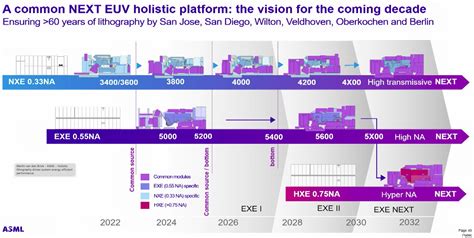
ASML’s High-NA EUV Roadmap:
ASML, a Dutch-based company, has been a pioneer in the development of EUV lithography systems. The company has set ambitious goals for its high-NA EUV technology, aiming to push the boundaries of semiconductor manufacturing. Here’s a summary of ASML’s high-NA EUV roadmap:
1. ASML’s current high-NA EUV system, the NXE:3400B, is designed to address the challenges of 7nm and 5nm process nodes. The system utilizes a 0.55 numerical aperture (NA) and is expected to be commercially available in 2021.
2. The company is actively working on the NXE:5000, a next-generation high-NA EUV system with a 0.7 NA. This system is expected to enable 3nm and 2nm process nodes, catering to the growing demand for advanced semiconductor manufacturing.
3. ASML is also investing in the development of a 1.0 NA system, which is anticipated to be a game-changer in the EUV lithography market. This high-NA system is expected to enable 1nm and beyond process nodes, paving the way for future innovations in the semiconductor industry.
Nikon’s High-NA EUV Roadmap:
Nikon, a Japanese company, has been a strong competitor to ASML in the EUV lithography market. The company has its own set of goals and strategies for high-NA EUV technology. Here’s a summary of Nikon’s high-NA EUV roadmap:
1. Nikon’s current high-NA EUV system, the NSR-S330C, is designed to address the challenges of 7nm and 5nm process nodes. The system utilizes a 0.55 NA and is expected to be commercially available in 2021.
2. The company is working on the NSR-S535C, a next-generation high-NA EUV system with a 0.7 NA. This system is expected to enable 3nm and 2nm process nodes, similar to ASML’s NXE:5000.
3. Nikon is also exploring the development of a 1.0 NA system, which is anticipated to be a significant leap in the EUV lithography market. This high-NA system is expected to enable 1nm and beyond process nodes, similar to ASML’s 1.0 NA system.
Comparison of ASML and Nikon’s High-NA EUV Roadmaps:
Both ASML and Nikon are investing heavily in the development of high-NA EUV technology, aiming to cater to the growing demand for advanced semiconductor manufacturing. Here’s a comparison of their roadmaps:
1. Process Nodes: Both companies are targeting similar process nodes, with ASML aiming for 1nm and beyond, while Nikon is also targeting 1nm and beyond.
2. NA: ASML is leading the way with its 1.0 NA system, while Nikon is following closely with its 0.7 NA system. Both companies are expected to develop 1.0 NA systems in the near future.
3. Commercial Availability: ASML and Nikon are expected to launch their next-generation high-NA EUV systems in 2021, catering to the 7nm and 5nm process nodes.
Conclusion:
The EUV lithography wars between ASML and Nikon are a testament to the rapid advancements in the semiconductor industry. Both companies are committed to pushing the boundaries of high-NA EUV technology, aiming to enable advanced process nodes for future semiconductor devices. As the competition heats up, we can expect to see even more innovative solutions from these industry leaders in the coming years.